You are currently viewing only those items made visible to the public. Click here to sign in and view the full catalogue.

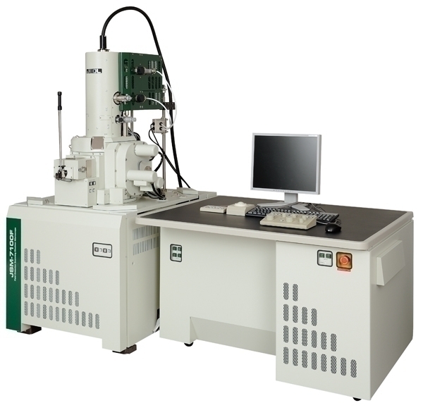
JSM-7100F Field Emission Scanning Electron Microscope
| MANUFACTURER | JEOL (manufacturer's website) |
|---|---|
| MODEL | JSM - 7100F |
| ACRONYM | FE-SEM |
| AVAILABILITY | Contact for Details |
|---|---|
| TRAINING | Training is required to use this item and we can arrange this if needed. |
| CALIBRATED | Yes, this item is calibrated. |
| CUSTODIAN | Keith Yendall |
|---|---|
| ADDITIONAL CONTACT | Sam Davis |
| Enquire about this item | |
| SITE | West Park |
Description
The FE-SEM consists of a high resolution field emission electron column. This allows for high magnification and resolution imaging using electrons.
Different Capabilities
- Large Depth Field
- UED
- LED
- USD
Specification
Performance
electron image (SEI):
- 1.2 nm guaranteed at 30 kV
- 3.0 nm guaranteed at 1 kV
Probe current: 1xl0^^–12^^ to 2xl0^^–7^^ A
Typical Applications
Collect large area EBSD maps at low magnifications without distortion Perform low kV imaging and analysis of highly magnetic samples. Large area EDS (EDX) is available for chemical composition analysis. Low Vacuum operation capability.
Upgrades
* Oxford Instruments X-max 80, Energy-dispersive X-ray spectroscopy (EDS).
* Oxford Instruments Nordlys, Electron Backscatter Diffraction (EBSD).
Retractable Back scatter detector,
Plasma Cleaner.
Future Upgrades
Item ID #.
Last Updated: 18th June, 2024